
ERCIM News 65April 2006Special theme: Space Exploration Contents This issue in pdf Subscription Archive: Next issue: July 2006 Next Special theme:
|
by Helen Mapson-Menard and Nick Waltham
The Imaging Systems Division at the Rutherford Appleton Laboratory are developing science-grade CMOS Active Pixel Sensors (APS) for future space science missions. Recent work has included successful testing of back-thinned devices, and the production of a new test APS chip.
Charge Coupled Devices (CCDs) are the current detector of choice for most scientific space instruments, for X-rays to infrared radiation. CMOS sensors promise significant advantages over today’s CCD technology. Firstly, modern CMOS processing enables smaller pixels than current science-grade CCDs, permitting more compact and lower mass instruments. Secondly, on-chip integration of the readout electronics minimises the size, mass and power requirements for ancillary control electronics and the associated problems of space-flight component procurement and radiation tolerance. Finally, deep sub-micron CMOS technology promises significantly higher radiation tolerance in the space environment compared to CCDs.
Our goal is the development of a large-format CMOS sensor with useful sensitivity in the extreme ultra-violet (EUV), for solar spectroscopy and imaging on ESA’s Solar Orbiter. Our CMOS APS development programme has been funded through a PPARC Rolling Grant to the Space Science and Technology Department at the Rutherford Appleton Laboratory.
We have developed a 4k x 3k pixel sensor with 5μm pixels fabricated on a 0.25 μm CMOS imager process. At EUV wavelengths the absorption depth in silicon is so shallow that the oxide layers on front-illuminated CMOS sensors absorb the photons before they reach the photodiodes. Our route to EUV sensitivity relies in adapting the back-thinning and rear-illumination techniques first developed for CCD sensors. Wafer samples of our APS have been thinned by e2v technologies with the aim of obtaining good sensitivity at EUV wavelengths.
|
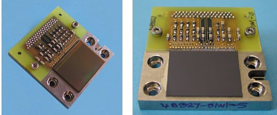
Figure 1 shows a photograph of two 4k x 3k sensors, one original sensor and one back-thinned. Each sensor is mounted on an invar block, and wire-bonded to a small printed circuit board (PCB) that carries ceramic decoupling capacitors for the power and DC bias supplies, and termination resistors for the LVDS clock receivers. A 51-way micro-D connector soldered to the underside of the PCB provides the connections interface.
|
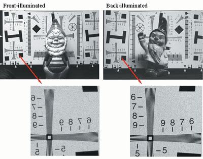
The 4k x 3k APS chips were successfully tested with front and back illumination, from 200 nm to 1000 nm. Test images obtained from both front and back illuminated sensors are reproduced in Figure 2. Both were obtained with sensors cooled to 273 K. The front illuminated image was taken in white light, whereas the back-illuminated image was obtained through a 50 nm wide narrow-band filter centred at 350 nm and an infrared blocking filter. It is important to note that the back-illuminated sensor would not be expected to work well at long wavelengths, because photons penetrate sufficiently to create electrons within the readout electronics rather than in the substrate from where they are collected by the photodiode. We have yet to attempt detailed characterization of the MTF performance of the back-illuminated sensor, but we have determined that the resolution is not significantly degraded compared to the front-illuminated sensor.
The next development is a test structure consisting of six arrays of 512 x 512 10 μm pixels. Each of the arrays has been given a different pixel design to allow verification of our models, and our progress towards optimizing a design for minimal system readout noise and maximum dynamic range. These sensors are also being back-thinned by e2v technologies for characterisation at EUV wavelengths. Once the test structure has been characterised, a new CMOS APS will be developed and back-thinned with the optimal pixel design for Solar Orbiter specifications.
Links:
RAL Imaging Systems homepage: http://www.sstd.rl.ac.uk/Divisions/Imaging_Systems.htm
ESA Solar Orbiter page: http://sci.esa.int/science-e/www/area/index.cfm?fareaid=45
Please contact:
Nick Waltham, CCLRC, UK
Tel: +44 1235 446500
E-mail: n.r.waltham![]() rl.ac.uk
rl.ac.uk